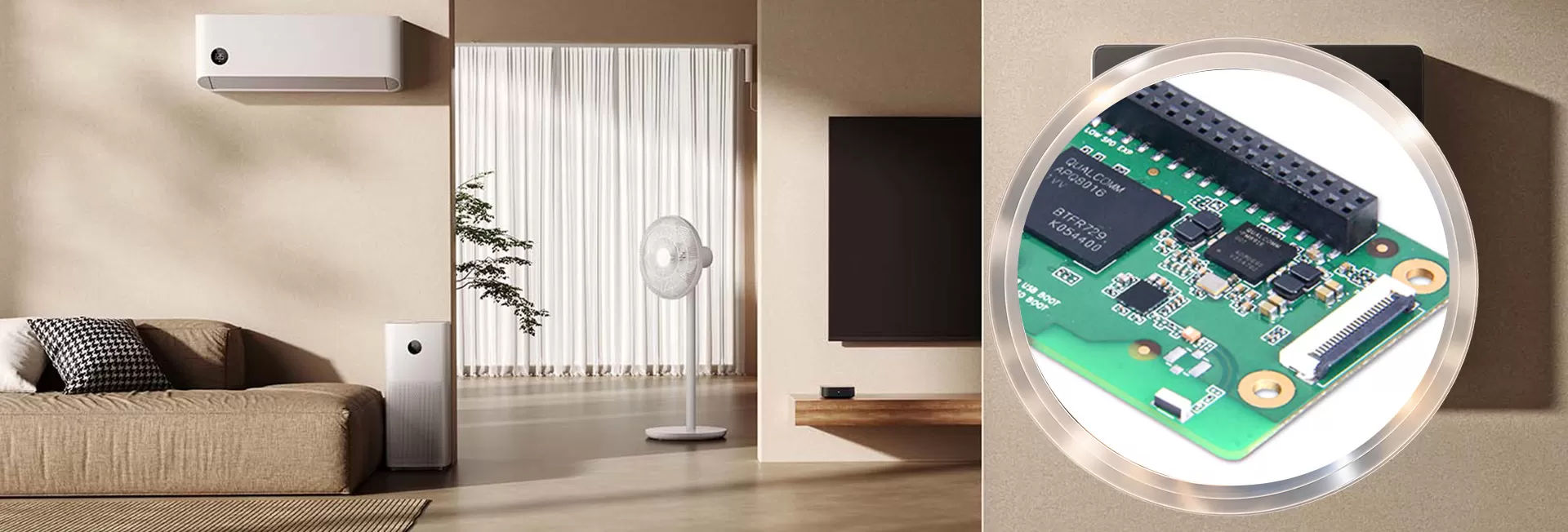
The quiet one behind cameras, locks and gateways is the Smart Home PCBA assembly. Miniaturization continues to make strides through SMT assembly technology, while stability remains essential for connected smart home electronics. KnownPCBA is a PCBA assembly manufacturer developing Smart Home PCB assembly solutions that bring compact design and stable assembly together.
Smaller electronics need precise SMT assembly without compromising the reliability expected from always-connected smart home devices.
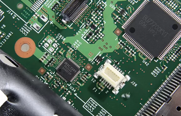
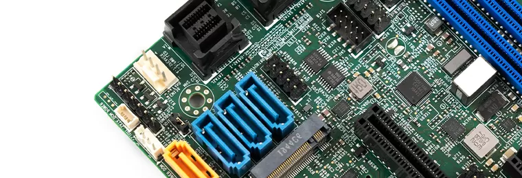
Smart home PCB assembly depends on high component integration inside increasingly compact layouts. MCUs, Wi-Fi chips and power modules are packed into small package designs through advanced SMT assembly.
MCU, Wi-Fi and power functions share very limited PCB space.
MCUs, Wi-Fi chips and power modules are placed close together. As the layout becomes denser, component position and SMT placement accuracy become increasingly important.
Compact packages support miniaturization but leave less room for placement error.
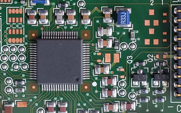
QFN, BGA and WLCSP packages support high-density smart home electronics. At this scale, even small SMD component movements can create significant assembly and layout problems.
Connector geometry and component height also influence the reflow process.
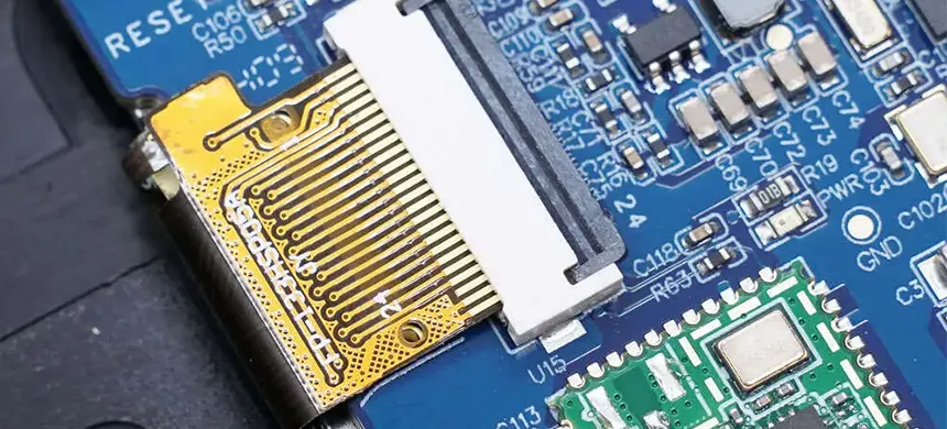
FPC connectors and BTB connectors add another layer of complexity. Device and component height can have a larger influence than expected when determining the appropriate SMT reflow profile.
As smart home PCBs become smaller, package size, placement accuracy, connector geometry and component height increasingly interact within the same SMT assembly process.
Share your Gerber files, BOM or assembly requirements with our team. We can help review component sourcing, SMT assembly details and production considerations before your project moves forward.
The key to this is really strict manufacturing control. KnownPCBA bridges prototyping and mass production through careful BOM sourcing and Surface Mount Technology (SMT) placement.
Fine-pitch assembly leaves little room for process variation.
Fine-pitch SMT assembly depends on controlled stencil design, solder paste volume and connector alignment. View Assembly Capabilities
Stencil apertures are adjusted to support stable solder paste deposition on compact smart home PCB layouts.
Paste volume is controlled to reduce tombstoning and hidden void risks.
Connectors and delicate interfaces are checked for alignment before final integration.
Operations Center Shenzhen KnownPCBA Technology Co.,LtdBldg D,Liantangkeng Industrial Area,Qianjin Road,Xixiang Street,Bao'an Dist.,Shenzhen City,Guangdong Province,518102,China.
| Have Question? Request a call back |