+86(755) 27944155 sales@knownpcba.com
Home Assembly Service PCBA Process
PCBA MANUFACTURING TECHNOLOGY

Our Main Manufacturing Technology of PCBA Process

Advanced PCBA manufacturing technology coveringsurface mount assembly, precision soldering andquality control process.
PCBA Process
01

Surface Mount Technology Process

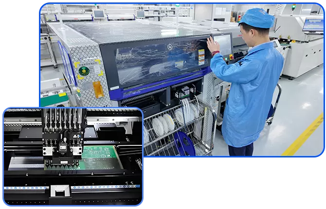
High precision SMT assembly ensures accuratecomponent placement and reliable solder joints.

Solder Paste Printing SPI Inspection Component Placement Reflow Soldering
Solder Paste Printing
Solder Paste Inspection (SPI)
Component Placement
Reflow Soldering
+ Process Details
The solder paste is precisely applied to the padsof the PCB with a laser steel mesh.

Before expensive components are mounted,a 3D SPI device checks the printed solder paste.It verifies volume, area and height to ensure quality.

The high-speed placement machine operates atextremely high speed.Vacuum suction tips precisely place small componentsonto solder pads with micrometer accuracy.

The PCB with attached components passes throughthe reflow soldering furnace.The four temperature zones include preheating,constant temperature, reflow and cooling.
PCBA MANUFACTURING TECHNOLOGY

Through Hole Insertion Technology Process

Reliable through-hole assembly technology improvesmechanical strength and connection stability for large components.
PCBA Process
02

Through Hole Insertion Technology Process

Improving mechanical reliability through preciseinsertion and soldering control for large electronic components.

Through Hole Insertion Large Components Wave Soldering Selective Soldering
Through Hole Insertion

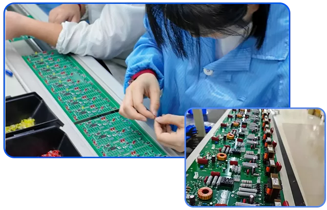
THT process is applicable to large-sized componentssuch as connectors and transformers to improvemechanical reliability.

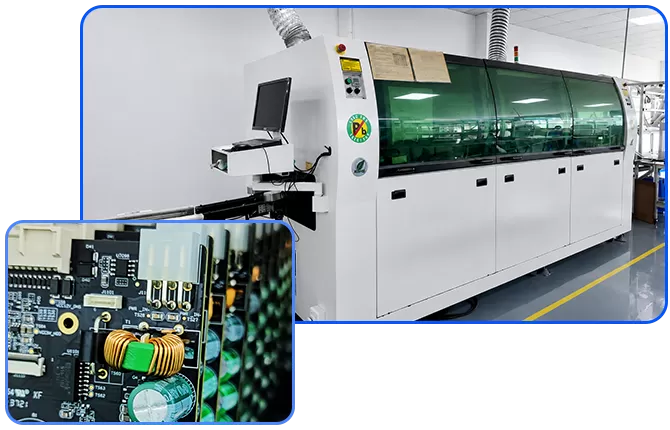
Wave Soldering

After THT insertion, the PCB passes througha wave of molten solder.The solder wets and fills pins and hole walls.Selective wave soldering is used for sensitive components.

+ Process Details
To improve the mechanical reliability,THT process is applicable to some large-sizedcomponents such as connectors and transformers.

After THT step, the board will pass througha wave of molten solder.The solder will wet and fill the pinsand the hole walls.

To protect sensitive components,we commonly use more preciseselective wave soldering.
PCBA MANUFACTURING TECHNOLOGY

Double In-line Package Technology Process

Reliable DIP assembly technology for through-hole ICcomponents and special electronic devices.
PCBA Process
03

Double In-line Package Technology Process

Reliable DIP assembly solution for IC componentswith dual-row pins and through-hole structures.

DIP Package IC Insertion Through-hole Components Wave Soldering
Manual or Automatic Insertion

DIP packaged chips, large electrolytic capacitors,transformers, pin headers and USB interfacesare inserted into corresponding PCB holes.

Wave Soldering

Similar to THT assembly,wave soldering is performed after DIP insertionto complete reliable solder connections.

+ Process Details
Some orders involve the assembly of ICswith pins on both sides.

Classic components such as NE555 timersand AT89C51 microcontrollers use DIP packageswith relatively large pin spacing.

Manual or automatic insertion machines installDIP packaged chips, large electrolytic capacitors,transformers, pin headers and USB interfacesinto corresponding PCB holes.

Like THT assembly,wave soldering is the following processafter DIP insertion.
Operations Center

Shenzhen KnownPCBA Technology Co.,Ltd

Bldg D,Liantangkeng Industrial Area,Qianjin Road,Xixiang Street,Bao'an Dist.,Shenzhen City,Guangdong Province,518102,China.

PCBA Process Tel:

+86 755 2794 4155

PCBA Process Fax:

+86 755 2794 4159

PCBA Process E-mail:

sales@knownpcba.com

Have Question?

Request a call back

Send Message
Name*
Email*
Company Name*
Address
Job Title
Phone Number