KnownPCBA has delivered over 30 electronic projects across a variety of applications, ranging from structural design to APP and hardware development.
Mr. Chen is the head of Hardware Engineering in KnownPCBA, who has 25 years of experience in hardware circuit design and the electronics industry.
AI Smart Device / APP / PCB Rendering
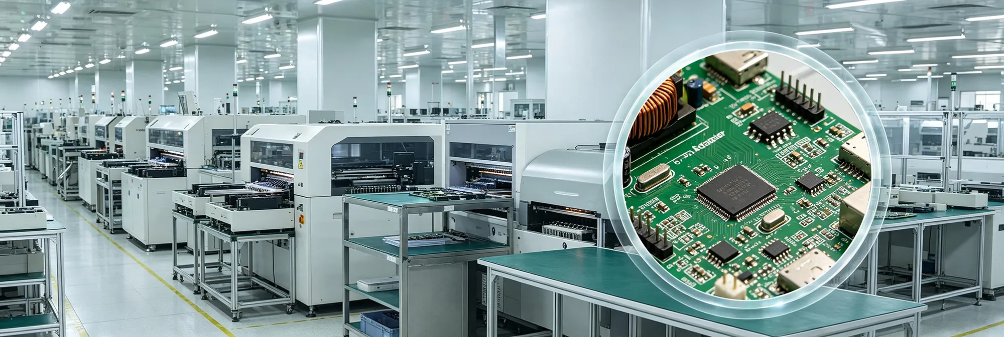
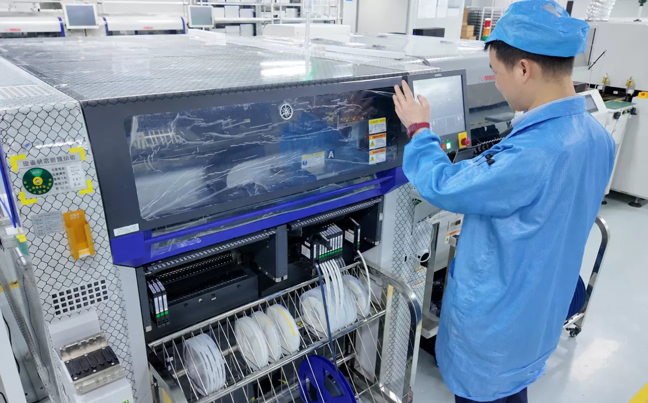
We have a modern intelligent manufacturing base equipped with fourhigh-speed SMT surface mount assembly lines and two DIP componentassembly lines. The product line includes the advanced MES manufacturingexecution system and automated logistics system. Our daily assemblycapacity exceeds forty thousand pieces, and our monthly productioncapacity remains stable at one million pieces.
In addition to the scale, we strictly keep good quality standards.Our AOI, 3D X-Ray, ICT, FCT full-function tests constitute completequality traceability network throughout the process. This ensures thatour on-time delivery rate can be above 99.8%.
Our mature supply chain management system and core material safetyinventory mechanism can guarantee delivery accuracy rate up to 98%.
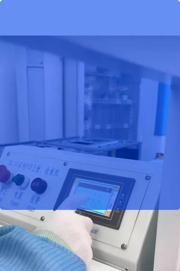
PCB size compatible with
L330×W250mm
Storage capacity 100 pieces
Compatible with SMEMA interface
Automatically adjustable track width.
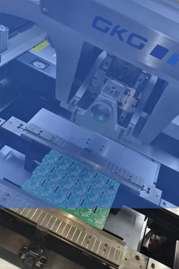
PCB size range:
50×50mm to 400×310mm
Thickness:
0.4~6mm
Repeat positioning accuracy:
±0.01mm
Printing accuracy:
±0.025mm
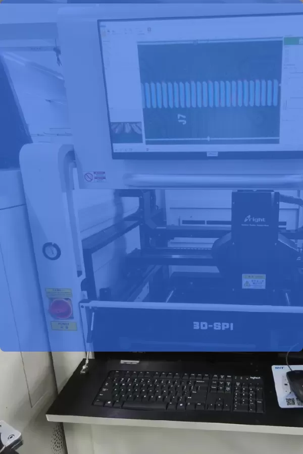
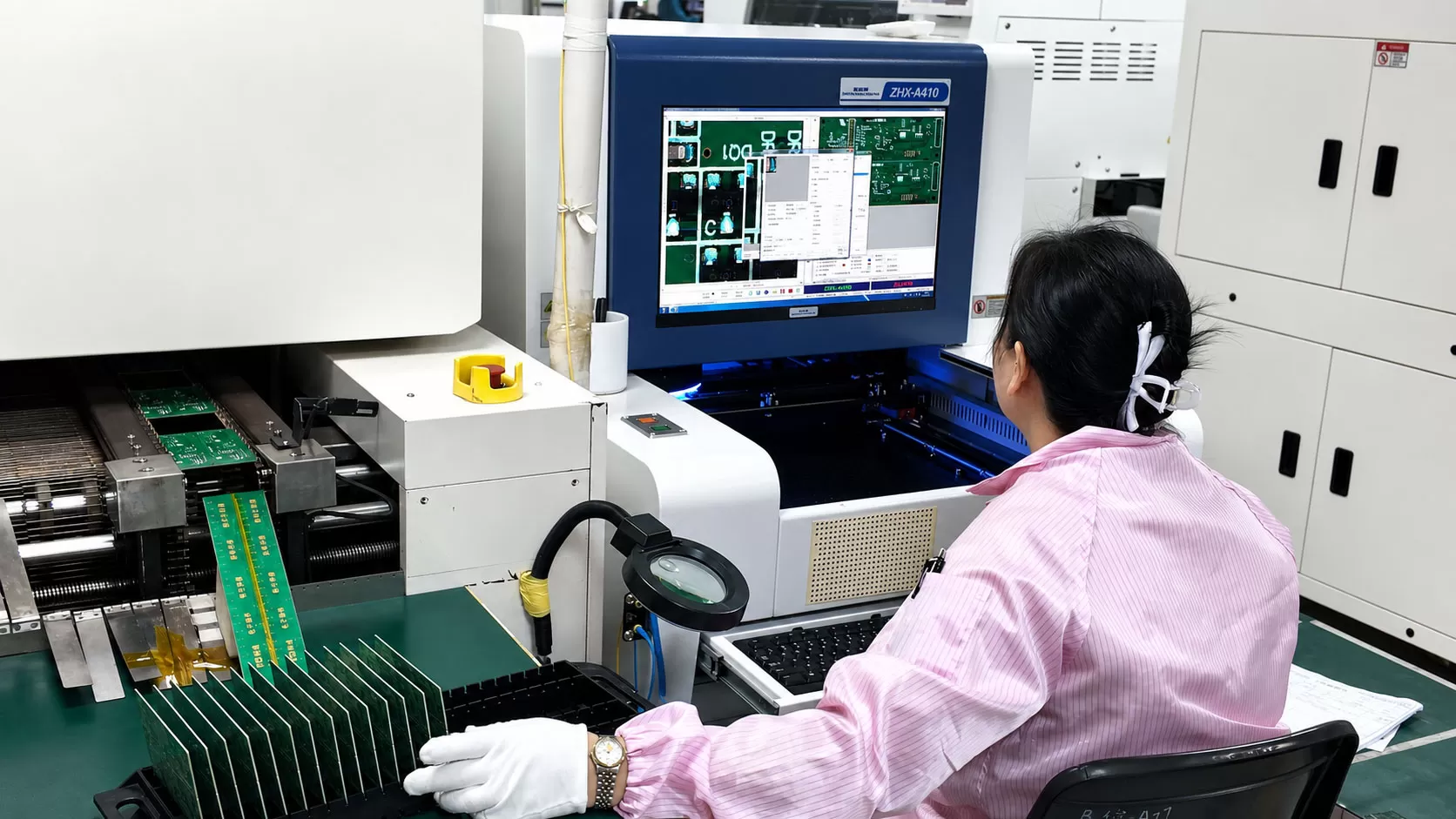
It can precisely detect key indicators such as solder paste thickness,area, and volume.
Compatible with the output inspection requirements of GKG G5 printers.
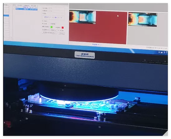
Equipped with a CCD color camera and RGB ring-shaped LED structurelight source, it precisely captures the details and defects of0201-sized micro components.
CCD COLOR CAMERA
RESOLUTION OPTIONS
RGB RING LED LIGHT
It leverages multi-algorithm fusion technologies including weightedimaging data difference analysis, color image comparison, OCR/OCV.
<10 ms
0201 COMPONENTS
IMAGE PROCESSING SPEED
<170 ms
SINGLE-FRAME
PROCESSING TIME
Full-dimensional coverage detection:It covers common SMT defects including solder paste printing defects,component missing, offset, standoff, solder joint bridging and voiding.
EQUIPMENT
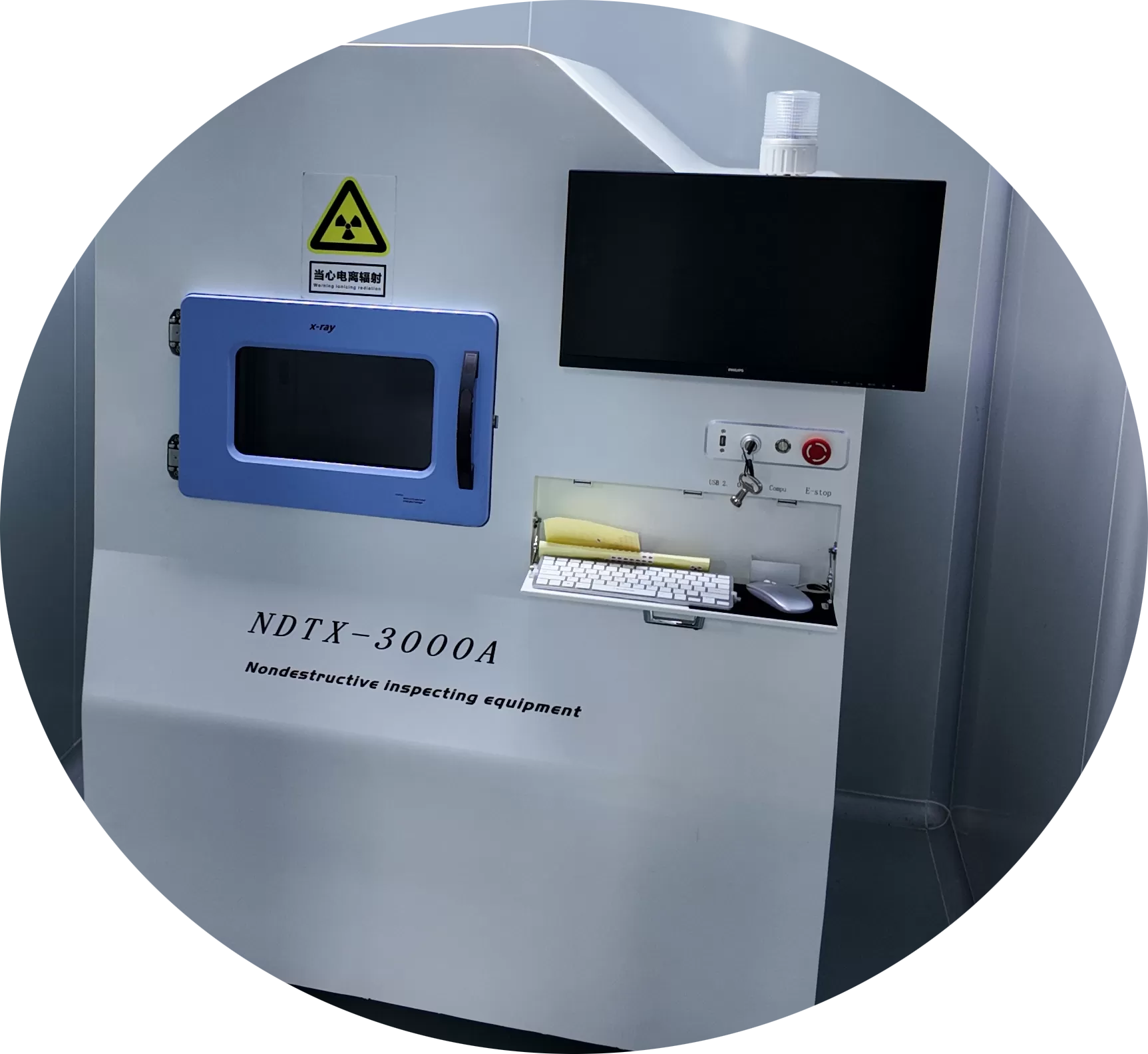
Advanced X-ray Inspection for Precision PCB Quality Control
Our X-ray Test Machine uses a 100KV closed-tube micro-focus X-ray sourcewith a focal size of only 5μm, enabling precise detection of hidden defectsinside PCB assemblies.
It accurately identifies issues such as BGA soldering defects, voidsbetween PCB layers, and other micro-level internal failures invisible toconventional inspection methods.
With up to 1200× total system magnification, a 1.3-megapixel CCD camera,and high-sensitivity image intensifier technology, it delivershigh-resolution inspection results.
Micro-focus X-ray Tube
Focal Spot Size
Maximum Magnification
Operations Center Shenzhen KnownPCBA Technology Co.,LtdBldg D,Liantangkeng Industrial Area,Qianjin Road,Xixiang Street,Bao'an Dist.,Shenzhen City,Guangdong Province,518102,China.
| Have Question? Request a call back |