
Short Lead Time, Design Guide and Quality Assurance
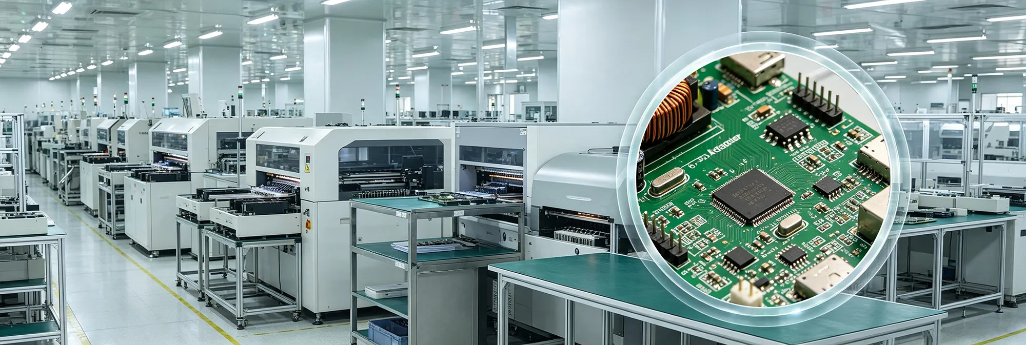
We are proud to be a China-based PCB assembly manufacturer supporting challenging PCB assembly prototyping and engineering builds for customers in the USA, Iran, Italy and other markets. We work closely with teams developing LED systems, AI hardware, medical electronics and new-energy products. Many of these PCB assembly projects have short launch cycles. Some need physical PCB prototypes in hand within 5 days.
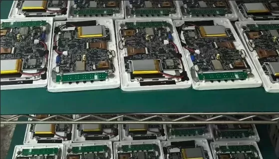
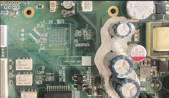
KnownPCBA keeps a fast-response route for urgent and lower-quantity PCB assembly work.
Our current PCB assembly production arrangement reserves around 10%–15% of capacity for fast-response work. For suitable PCB assembly processing, the production-line changeover can be completed in about 15–30 minutes.
In turnkey PCB assembly prototype projects, we offer a wide range of component purchasing solution. You may already own the MCU but need us to buy the remaining passive parts. Another PCB assembly project may have a difficult sensor, or one IC that must come from an approved source. Full turnkey works for some. Partial sourcing is better for others. We are comfortable with both.
We coordinate the board, material and build. This is usually simpler when the customer wants one team to own the manufacturing side instead of coordinating several vendors.
Keep the expensive or controlled devices on your side. We can source the rest. In real prototype work, this is quite common and often easier for both teams.
If your material is already purchased, that is fine. We focus on getting it through incoming handling and the assembly process without creating another unnecessary procurement step.
Select the inspection, testing or manufacturing-control topic you need to review.
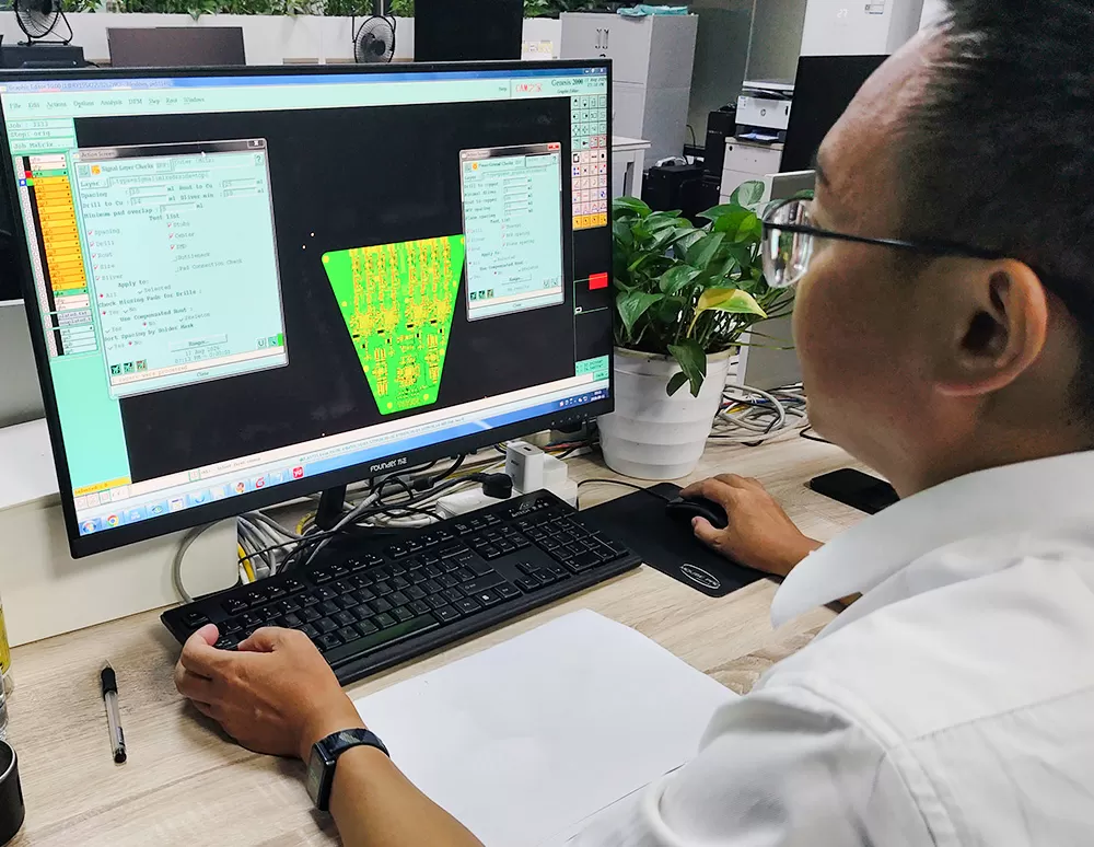
With complete Gerber, BOM, pick-and-place, assembly drawing and test data, our engineers review the build against the real limits of our own SMT, assembly and test lines.
These are the issues that cause real production trouble: parts that cannot be placed, test points that cannot be reached, rework, delay and extra cost.
We close those risks before the build reaches the line.
You receive a clear status: Ready to Build, Conditional Release, or Hold for Decision.
Every issue is numbered and linked to the exact reference designator, PCB layer or affected location.
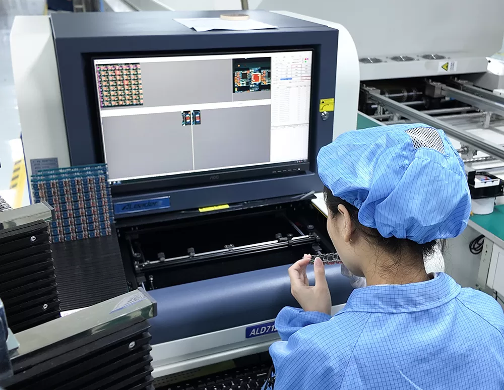
Problems are caught at the stage where they are still cheaper and easier to correct. Your prototype reaches engineering validation with fewer assembly variables left unexplained.
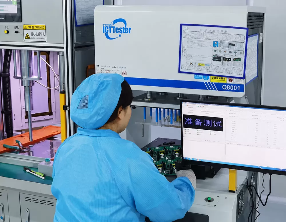
We can support Flying Probe, ICT or FCT according to the project purpose. A first engineering build may only need connectivity checks. Another board may already have a functional procedure, firmware and acceptance criteria.
We use the level of test that helps answer the engineering question behind the prototype. A small build should not be forced into a full production test system when it does not need one yet.
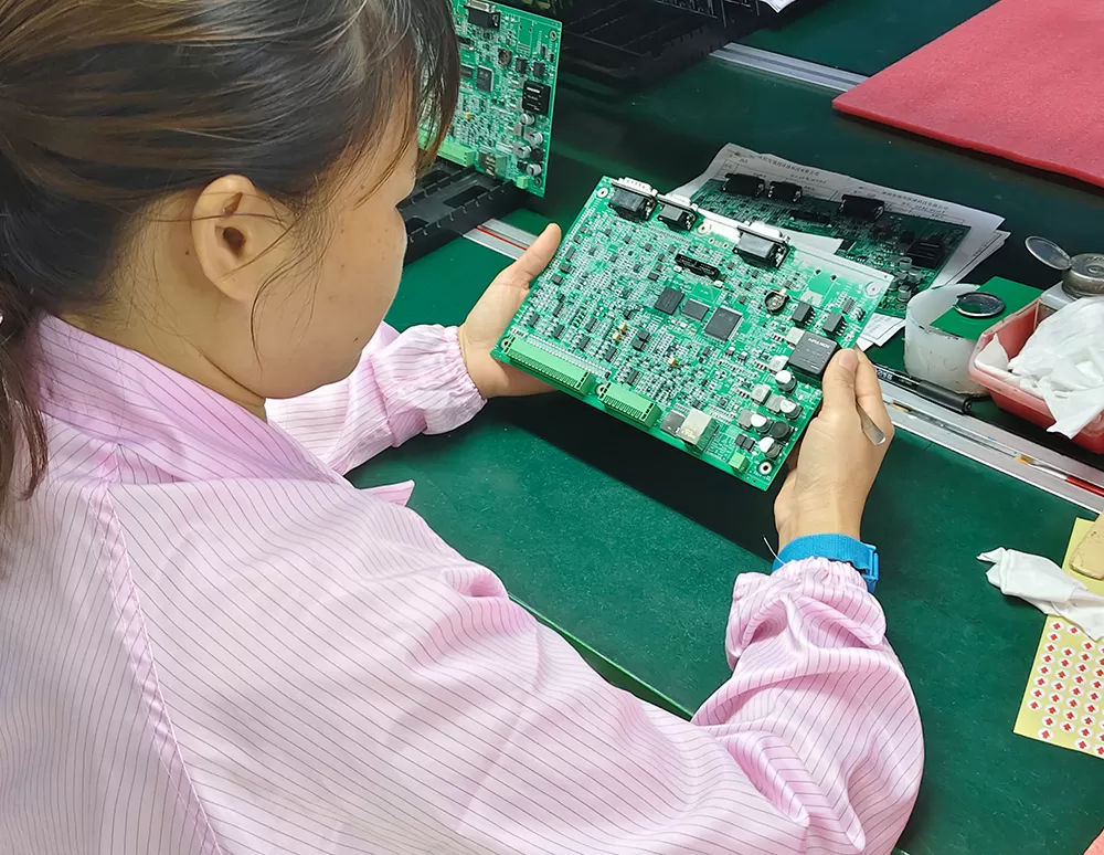
Every PCB version we assemble keeps its own manufacturing history — material lots, process settings, inspection results, test records and engineering changes.
When the same PC board comes back for a second fabrication and assembly build, we do not start from zero. The previous build already tells us what worked, what changed and where extra attention was needed.
The value increases when a prototype moves into production. It is one reason we have been able to support customers in demanding industries for more than 10 years, including automotive programs under IATF 16949 requirements and medical projects under ISO 13485 requirements.
The second build should be easier than the first.
We identify the handoff points during project review and keep the build under one manufacturing control: same site, same process file, same inspection criteria, same engineering team and the same traceability record. No cross-factory transfer. No outsourced handoff. One accountable team.
Fine-pitch SMT and high-current through-hole parts are reviewed together before release, including assembly sequence and second-reflow exposure.
Manual soldering, selective soldering or pin-in-paste is selected by component and board design. Selective-solder parameters are controlled for repeat builds.
Through-hole joints follow the agreed IPC-A-610 class, including vertical-fill requirements and the inspection method used for the build.
Same site, process file, engineering team and traceability record. No outsourced handoff between SMT and through-hole stages.
Where practical, prototypes use the same soldering route and acceptance criteria planned for volume production.
A successful prototype should give you manufacturing evidence that can move forward with the product, not a one-off result that has to be proven again.
Most purchasing teams do not need these parameters first. Engineers sometimes do. They stay available here without interrupting the main prototype purchasing path.
Our current engineering guideline treats 0.1 mm trace width as a process-limit condition. Where the design allows it, about 0.15 mm gives more manufacturing margin. For routing, 45° or curved corners are preferable to sharp acute angles.
Pads closer than 0.5 mm to a finished edge create more risk during fabrication and handling. Our current recommendation is at least 0.75 mm for components or through-hole features, with about 1 mm preferred where the mechanical design permits. A 3–5 mm process edge may also be needed.
For component pitch below about 0.5 mm, the current guideline references a solder-mask dam around 0.075 mm where the board construction permits it. Stencil aperture adjustment may also be used when solder volume needs tighter control.
Vias below about 0.2 mm and annular-ring values below about 0.15 mm deserve extra review. The existing manufacturing guide also uses approximately 0.25 mm as a recommended minimum mechanical-hole reference.
The current guideline recommends at least three diagonal global fiducials with approximately 1 mm bare-copper diameter. Local fiducials should maintain enough clearance from nearby components for stable optical recognition during placement.
Send us the Gerber, BOM, quantity and assembly information you already have. If functional testing or programming matters, tell us early. We can work through the rest with you.
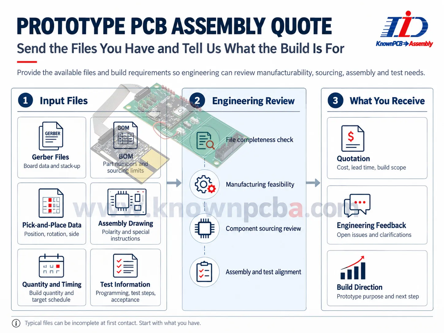
We have been in enough challenging prototype projects to know that the first plan is not always the final plan. Parts change. Deadlines move. Engineers find things after power-on. That is normal product development. We are proud to be the manufacturing side that stays useful when those changes happen, not only when everything is already perfect.
Request a Prototype PCB Assembly QuoteProven by 7 industries, 4000+ customer projects
Please contact us at sales@knownpcb.com, ask for engineering support here or use the form below to reach out to KnownPCB | Get In Touch Today |