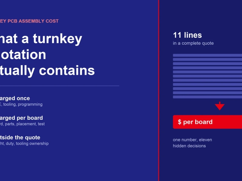

| Custom printed circuit boards can range from surprisingly affordable to expensive depending on design choices, materials, volume, testing needs, and assembly complexity. Understanding what drives PCB manufacturing cost early helps you make smarter engineering decisions before requesting PCB assembly quotes. This guide explains the main cost factors and practical ways to control custom circuit board cost without weakening performance or reliability. | 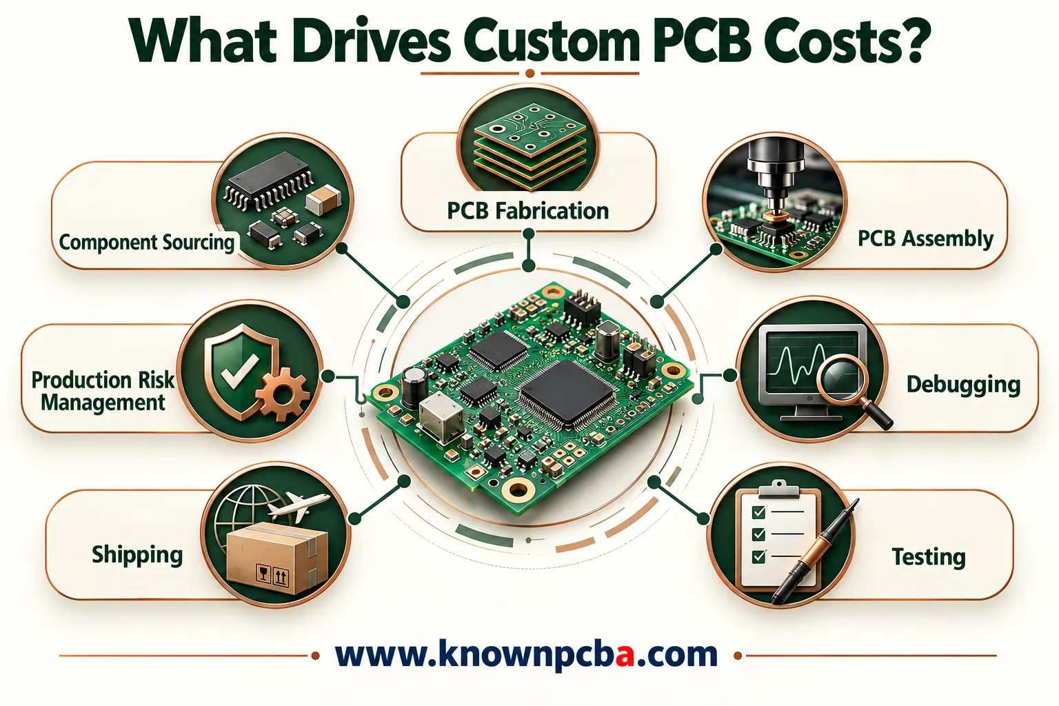 |
What Really Affects Custom PCB Pricing?
Custom PCB pricing is shaped by the bare board, the components installed on it, the production process, and the quality assurance required. A simple two-layer prototype with common parts will usually cost less than a dense multilayer board with fine-pitch components, controlled impedance, and extensive inspection.
Cost is a combination of fabrication, component sourcing, assembly, setup, testing, shipping, and production risk. Focusing only on the bare-board price can hide expenses caused by difficult assembly, unavailable components, or special handling requirements.
An activity-based approach offers a useful theoretical foundation: estimate cost from the manufacturing activities a design requires, rather than treating every PCB assembly as an equivalent unit. N. S. Ong’s research applies this approach to early PCB assembly cost estimation. [4]
Board Design Choices That Influence Fabrication Cost
The physical design of a PCB is a major cost driver. Manufacturers consider how difficult the board will be to fabricate consistently. Increasing density, tighter tolerances, and specialized structures can require additional processing and closer control.
Layer Count and Stackup
Two-layer boards are typically easier and less expensive to fabricate than multilayer boards. Additional layers increase material use and processing complexity. Sequential lamination, when required by an HDI structure, adds further steps. More layers may be necessary for signal integrity, power distribution, or routing density, but the stackup should match the actual design requirements.
Board Size, Shape, and Panel Utilization
Larger boards consume more laminate and panel space. Irregular outlines, cutouts, slots, and complex routing can increase machining time or reduce panel utilization. A smaller board does not automatically cost less if achieving that size requires finer features or more layers.
Trace Width, Spacing, and Via Structures
Fine traces, tight spacing, small drilled holes, microvias, blind vias, buried vias, and high drilling aspect ratios can increase fabrication difficulty. Use these features when they provide a necessary electrical or mechanical benefit, and confirm the manufacturer’s capabilities before finalizing the layout.
IPC-2221B provides a general design framework covering materials, physical configuration, electrical properties, component placement, and testability. It supports manufacturability decisions but does not provide a universal PCB pricing formula. [1]
Materials and Finishes Make a Practical Difference
Standard FR-4 is common in many applications. High-frequency laminates, high-temperature materials, flexible circuits, rigid-flex constructions, and metal-core boards can increase cost. These options may be necessary for RF performance, thermal management, mechanical flexibility, or compact packaging.
Copper weight: Heavier copper can support current carrying and heat spreading, but it also changes etching requirements and achievable feature sizes. Copper thickness should be selected together with trace geometry and thermal requirements.
Controlled impedance: Specified impedance tolerances require coordination among layout, laminate properties, copper geometry, and the stackup. Verification requirements can also affect the quote.
Surface finish: Select finishes according to solderability, storage conditions, component pitch, and the intended environment. The lowest initial finish price may not deliver the lowest overall cost if it creates assembly or reliability problems.
Printed Circuits Handbook provides broad technical background on PCB materials, fabrication processes, assembly, and testing—the engineering foundations behind these tradeoffs. [2]
How Does Assembly Complexity Change the Final Cost?
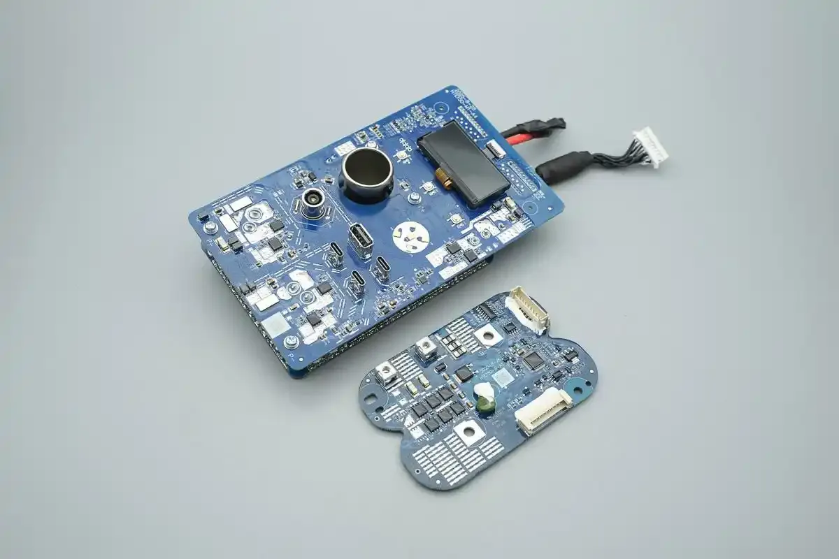
Assembly can contribute as much as, or more than, bare-board fabrication to the final PCB assembly cost. Components must be sourced, verified, placed, soldered, and inspected. Some products also need programming, coating, or functional testing.
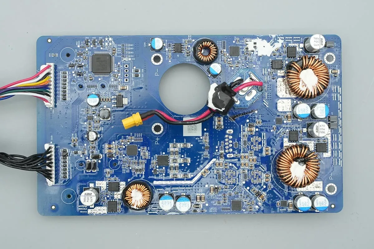
SMT supports efficient automated production, but small packages, fine-pitch ICs, BGAs, and dense placement increase process demands. Through-hole components may require manual insertion, wave soldering, or selective soldering. Mixed SMT and through-hole designs can involve multiple assembly stages.
- Component count: More placements increase machine time and inspection workload.
- Unique part numbers: More BOM line items increase sourcing, verification, and feeder setup work.
- Package type: BGAs, fine-pitch devices, and tiny passives can require tighter process control and specialized inspection.
- Double-sided assembly: Components on both sides generally introduce additional printing, placement, and soldering operations.
- Special handling: Moisture-sensitive devices, odd-form parts, conformal coating, and programming add process steps.
Texas Instruments’ guidance for 0.5 mm package-on-package designs illustrates why fine-pitch assembly requires coordinated decisions about pads, vias, stencil design, solder paste, and reflow. Its package-specific dimensions should not be applied indiscriminately to other devices. [3]
For low-cost PCB assembly, simplify unnecessary part variety, use readily available components, leave suitable assembly access, and choose footprints compatible with the intended production process.
 |  |
Prototype Volume Versus Production Volume
Quantity changes the economics of fabrication and assembly. Engineering review, tooling, stencil preparation, machine programming, and procurement effort are spread across relatively few boards in a prototype run. Larger orders can distribute these setup costs across more units.
That is why PCB assembly quotes can differ substantially at 5, 50, 500, and 5,000 units, even when the design is identical. Component price breaks and production efficiency can also affect unit cost.
Ordering more boards before validation introduces inventory and redesign risk. Prototype first, verify the design and assembly process, then scale when performance and the supply chain are sufficiently stable.
Testing, Inspection, and Documentation Add Value
Clear manufacturing data improves quoting and execution. Provide fabrication files, drill data, stackup requirements, a BOM, pick-and-place data, assembly drawings, polarity information, test procedures, and revision identifiers as applicable. Incomplete or inconsistent files can create delays, incorrect assumptions, and extra engineering work.
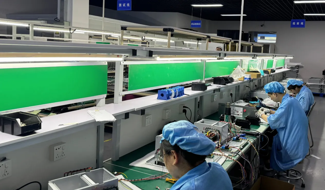
Inspection and testing help identify manufacturing defects before shipment. The appropriate combination depends on component packages, circuit complexity, accessibility, production volume, and product requirements.
|  |
Why Do PCB Assembly Quotes Differ Between Suppliers?
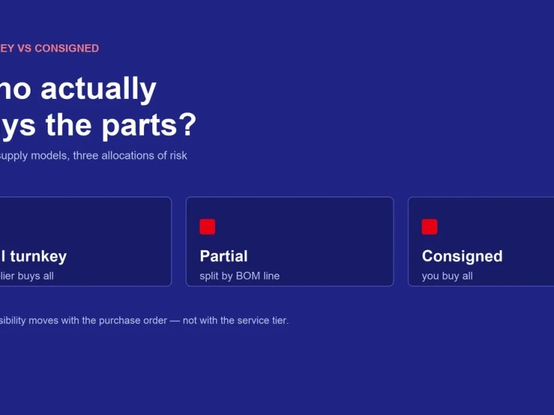
Suppliers use different equipment, sourcing channels, labor models, minimum order policies, and quoting assumptions. One quote may include fabrication, components, assembly, stencils, inspection, and testing, while another covers only assembly labor.
Compare quotes against the same revision, quantities, delivery requirements, and acceptance criteria. Confirm component sourcing responsibilities, substitutions, excess parts, setup charges, tooling, testing, shipping, and how defects or rework will be handled.
The cheapest quote may create a higher total cost if it leaves essential work outside the scope. A useful comparison considers both the quoted price and the supplier’s ability to deliver the agreed product consistently.
Practical Ways to Reduce PCB Cost Without Cutting Corners
Cost reduction works best during design. Before requesting PCB assembly quotes, review the following checklist:
- Confirm the layer count. Use the stackup needed for routing, power delivery, EMI control, and signal integrity.
- Use standard fabrication capabilities. Confirm practical trace, spacing, hole, and thickness options with the manufacturer.
- Choose available components. Review lifecycle status, lead times, and technically suitable alternatives.
- Reduce unnecessary part variety. Consolidate values and packages where electrical requirements permit.
- Allow assembly and test access. Consider placement, soldering, inspection, probing, and rework.
- Justify special processes. Specify advanced vias, materials, finishes, and coatings when the application requires them.
- Supply complete, consistent files. Keep the BOM, drawings, placement data, and fabrication package on the same revision.
- Validate before scaling. Resolve design and process issues before committing to a larger production order.
The Total Cost Is Bigger Than the Board Price
The true cost of PCB assembly can include engineering time, revisions, component overages, freight, customs, incoming inspection, troubleshooting, rework, and schedule impact. A board that costs slightly more to manufacture may be less expensive overall if it avoids repeated production problems.
Every product has different priorities. A consumer device, industrial controller, LED product, IoT sensor, and RF module may require different materials, testing, and process controls. The right cost strategy follows performance requirements, expected volume, reliability needs, and product lifecycle.
Key Takeaway
Custom PCB cost is driven by design complexity, materials, component sourcing, assembly, testing, documentation, and quantity. To obtain meaningful PCB assembly quotes, provide complete files and compare equivalent scopes. Design for manufacturability early, validate prototypes, and scale when the board and production process are ready.
References and Technical Background
These publications provide general engineering and cost-estimation background. They do not establish supplier-specific prices. The IPC link below provides the cited edition’s official contents preview; production requirements should identify the applicable standard and revision.
- IPC-2221B: Generic Standard on Printed Board Design.
Author / developing body: IPC-2221 Task Group (D-31b), Rigid Printed Board Committee (D-30), IPC. November 2012.
Technical background: PCB design, materials, configuration, component placement, and testability.
Official IPC contents preview (PDF) - Printed Circuits Handbook, Seventh Edition.
Authors / editors: Clyde F. Coombs, Jr. and Happy Holden. McGraw-Hill Education, 2016.
Technical background: Printed circuit materials, fabrication, assembly processes, and testing.
Publisher’s book page - PCB Design Guidelines for 0.5mm Package-on-Package Applications Processor, Part I.
Authors: K. Gutierrez and Keven Coates. Texas Instruments, Application Report SPRABB3, June 2010.
Technical background: Fine-pitch manufacturability, fabrication limits, vias, stackup, and assembly coordination.
Texas Instruments application report (PDF) - Manufacturing Cost Estimation for PCB Assembly: An Activity-Based Approach.
Author: N. S. Ong. International Journal of Production Economics, Volume 38, Issues 2–3, pages 159–172, 1995.
Theoretical background: Estimating PCB assembly cost from manufacturing activities during early design.
Article DOI and publisher link